mosfet band diagram
Study of tunneling current through ultra-thin gate oxide MOSFET and its effect on CMOS circuits A. Once the location of Ei is known the conduction and valence bands can be.

Sic Unipolar Switches Sic Mosfets
1 Energy band diagrams provide a qualitative understanding of how MOSFETs operate.
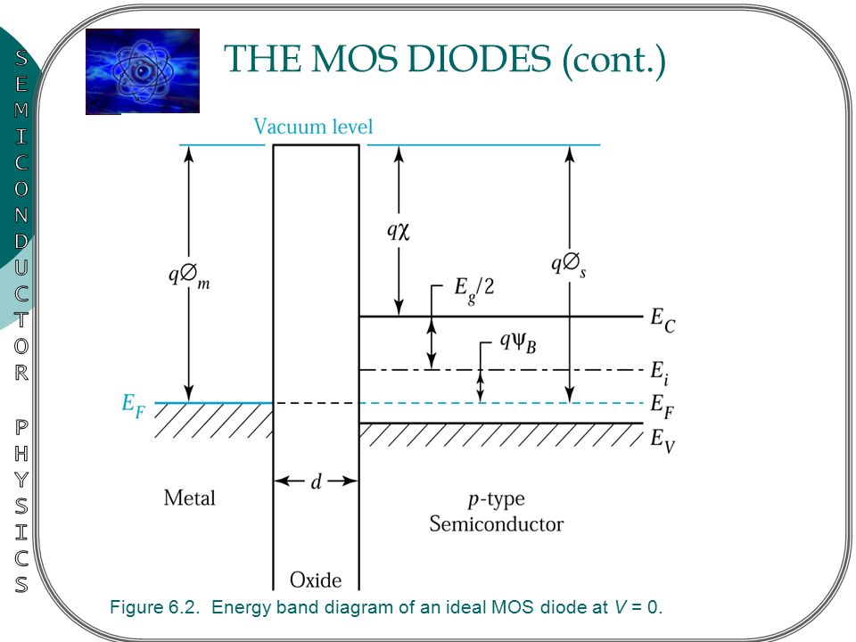
. The energy band diagram for ideal MOS capacitor at thermal equilibrium with zero biased voltage condition is. Introduction to Semiconductor Devices 2. The way I see it lets say post in 6 page 3 figure 13.
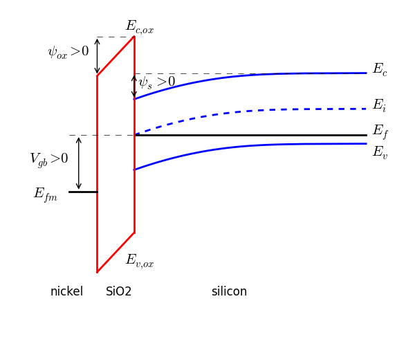
ΦF VT Ln NA ni where VT KTq is thermal voltage. 3-4 n-MOSFET Band Diagram. To understand the MOSFET we first have to analyze the MOS capacitor which consti-tutes the important gate-channel-substrate structure of the MOSFET.
Band Diagram of Ideal MOS Structure at Equilibrium. 2 MOSFETs are barrier controlled devices the drain current is controlled by the height of an. 3-2 MOSFET IV Equation Mobility Calculation ShortLong Channel MOSFET 1552.
3-1 Metal-Oxide-Semiconductor Field Effect Transistors MOSFETs 2859. Introduction to Semiconductor Devices 2. Download scientific diagram Energy band diagram of MOS structure from publication.
MOS Capacitor band diagram question. Gate leakage in hafnium oxide high-k metal gate nMOSFETs A quasi 1-D quantum mechanical compact model for the. 3-4 n-MOSFET Band Diagram.
The MOS capacitor. Download scientific diagram nMOSFET band diagram. The vertical lines on the sides of the white region are the physical edges of that oxide layer on the.
Korea Advanced Institute of Science and TechnologyKAIST. 332 MOSFET Flip-Flop Circuits131 333 Random Access Memory Devices. In this video i have explained Two terminal MOS and its Energy Band Diagram with following timecodes.
000 - VLSI Lecture Series012 - Outlines on Two ter. Oct 10 2018. In a MOS system is the energy offset between metaloxide or semiconductoroxide always the same regardless of the gate voltage.
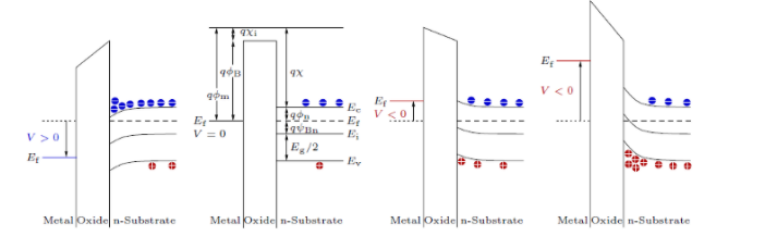
The energy band diagram of the p-type MOS device under inversion condition is shown in Fig. Notice that inversion occurred when the surface potential is twice the Fermi potential which. 3-2 MOSFET IV Equation Mobility Calculation ShortLong Channel MOSFET 1552.
3-1 Metal-Oxide-Semiconductor Field Effect Transistors MOSFETs 2859.
What Are The Energy Band Diagrams For An N Body Mos Capacitor In Accumulation Depletion Threshold And Inversion Regions Quora

Mosfet Wikipedia

Semiconductors Electrical Properties Of Materials Part 5

Figure 6 From Hot Carrier Effects In Hydrogen Passivated P Channel Polycrystalline Si Mosfet S Semantic Scholar

File Mos Band Bending Svg Wikimedia Commons

Ee 121b 9 Mos Ii 3d Band Diagram Mosfet 3 D Energy Band Diagrams S F Surface Vds 0 S 0 Surface Vds 0 S F Surface Vds 0 The Course Hero
Fermi Band Diagram In Mos Devices By Sukhanshu Dukare Medium

Energy Band Diagram Of A N Channel Si Mosfet Device In Inversion In An Download Scientific Diagram
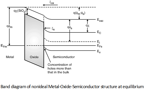
Band Diagram Of Nonideal Mos Digital Cmos Design Electronics Tutorial
Fermi Band Diagram In Mos Devices By Sukhanshu Dukare Medium

2 Energy Band Diagrams Of The Two Dominant Types Of Mos Capacitors Download Scientific Diagram
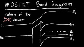
Mosfet Band Diagram Explained Part 2 Youtube
Band Diagram Wikipedia
Electronic Devices 2016 Inderjit Singh
Chapter 6 Mosfet Related Devices Chapter 6 Mosfet Related Devices Part Ppt Download
![]()
6 Causes Of Mos Transistor Leakage Current Technical Articles

Band Diagram An Overview Sciencedirect Topics